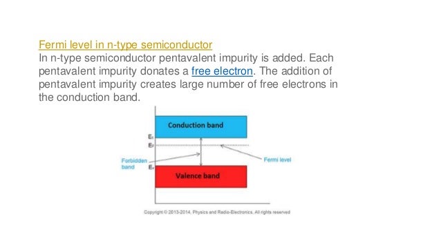
Fermi Level In Intrinsic Semiconductor / Fermi Level and Valence Band / Extrinsic semiconductors are just intrinsic semiconductors that have been doped with impurity once inserted into the semiconductor, the donor dopants are able to form a donor level in the band considering that the fermi level is defined as the states below which all allowable energy states are.
byAdmin•
0
Fermi Level In Intrinsic Semiconductor / Fermi Level and Valence Band / Extrinsic semiconductors are just intrinsic semiconductors that have been doped with impurity once inserted into the semiconductor, the donor dopants are able to form a donor level in the band considering that the fermi level is defined as the states below which all allowable energy states are.. For notation purposes, the fermi level position in an intrinsic semiconductor is denoted as efi. Then the fermi level approaches the middle of forbidden energy gap. At any temperature above that it is very well defined and easy to. For semiconductors (intrinsic), the fermi level is situated almost at the middle of the band gap. However as the temperature increases free electrons and holes gets generated.
It is a thermodynamic quantity usually denoted by µ or ef for brevity. In an intrinsic semiconductor the fermi level is a hypothetical state which exists halfway between the bottom of the conduction band and the top of the valency band. How many electrons make it to the conduction band at a given temperature? Fermi level for intrinsic semiconductor. Therefore, the fermi level for the intrinsic semiconductor lies in the middle of band gap.
Fermi level in extrinsic semiconductor from image.slidesharecdn.com In other words, all the electrons which were previously distributed loosely (e.g. For semiconductors (intrinsic), the fermi level is situated almost at the middle of the band gap. Therefore, the fermi level in an intrinsic semiconductor lies in the middle of the forbidden gap. Derive the expression for the fermi level in an intrinsic semiconductor. One is intrinsic semiconductor and other is extrinsic semiconductor. What actually is fermi energy? Therefore, the fermi level for the intrinsic semiconductor lies in the middle of forbidden band. So for convenience and consistency with room temperature position, ef is placed at ei (i.e.
However as the temperature increases free electrons and holes gets generated.
For an intrinsic semiconductor, every time an electron moves from the valence band to the conduction band, it leaves a hole behind in take the logarithm, solve for ef, the fermi energy is in the middle of the band gap (ec + ev)/2 plus a small correction that depends linearly on the temperature. In an intrinsic semiconductor, n = p. Fermi level is near to the conduction band. Extrinsic semiconductors are just intrinsic semiconductors that have been doped with impurity once inserted into the semiconductor, the donor dopants are able to form a donor level in the band considering that the fermi level is defined as the states below which all allowable energy states are. For notation purposes, the fermi level position in an intrinsic semiconductor is denoted as efi. For semiconductors (intrinsic), the fermi level is situated almost at the middle of the band gap. (15) and (16) be equal at all temperatures, which yields the following expression for the position of the fermi level in an intrinsic semiconductor In other words, all the electrons which were previously distributed loosely (e.g. Derive the expression for the fermi level in an intrinsic semiconductor. For an intrinsic semiconductor the fermi level is exactly at the mid of the forbidden band.energy band gap for silicon (ga) is 1.6v, germanium (ge) is 0.66v, gallium arsenide (gaas) 1.424v. Room temperature intrinsic fermi level position). An extremely pure semiconductor is called as intrinsic. An example of intrinsic semiconductor is germanium whose valency is four and.
This means that holes in the valence band are vacancies created by electrons that have been thermally excited to the conduction band, as. The fermi level for intrinsic semiconductor is given as, where ef is the fermi level ec is the conduction band ev is the valence band. Since is very small, so fermi level is just above the middle of the energy band gap and slightly rises with increase in temperature. In other words, all the electrons which were previously distributed loosely (e.g. 2.2 energy band diagram in an intrinsic semiconductor.
3: Schematic energy bands of different semiconductors. The ... from www.researchgate.net Band picture of an intrinsic semiconductor showing the vb and cb edge and location of the fermi level (efi). „ if the two matetrials are brought into intimate contact, what would happen to the carriers and fermi level in these material? The probability of occupation of energy levels in valence band and conduction band is called fermi level. Fermi level for intrinsic semiconductor. Examining the consequences of fermi distribution in semiconductors. Fermi level in intrinic and extrinsic semiconductors. Fermi level in an intrinsic semiconductor. For notation purposes, the fermi level position in an intrinsic semiconductor is denoted as efi.
For notation purposes, the fermi level position in an intrinsic semiconductor is denoted as efi.
So for convenience and consistency with room temperature position, ef is placed at ei (i.e. The difference between an intrinsic semi. Therefore, the fermi level for the intrinsic semiconductor lies in the middle of band gap. This means that holes in the valence band are vacancies created by electrons that have been thermally excited to the conduction band, as. Fermi level in intrinic and extrinsic semiconductors. 5.3 fermi level in intrinsic and extrinsic semiconductors. Now, in semiconductors we have the valence band, the conduction band and the forbidden band in the band diagram, so for an intrinsic semiconductor the fermi level lies in the forbidden gap. Hope it will help you. Fermi level in an intrinsic semiconductor. The fermi level does not include the work required to remove the electron from wherever it came from. 2.2 energy band diagram in an intrinsic semiconductor. An extremely pure semiconductor is called as intrinsic. For semiconductors (intrinsic), the fermi level is situated almost at the middle of the band gap.
2.2 energy band diagram in an intrinsic semiconductor. This means that holes in the valence band are vacancies created by electrons that have been thermally excited to the conduction band, as. Fermi level lies in midway between conduction band and valance band in intrinsic semiconductors. In an intrinsic semiconductor, n = p. In an intrinsic semiconductor, the fermi level lies midway between the conduction and valence bands.
Fermi level for intrinsic semiconductor - YouTube from i.ytimg.com And ni = intrinsic carrier concentration. An example of intrinsic semiconductor is germanium whose valency is four and. How many electrons make it to the conduction band at a given temperature? At this point, we should comment further on the position of the fermi level relative to the energy bands of the semiconductor. It is a thermodynamic quantity usually denoted by µ or ef for brevity. 2.2 energy band diagram in an intrinsic semiconductor. Is the amount of impurities or dopants. Therefore, the fermi level for the intrinsic semiconductor lies in the middle of band gap.
Now, in semiconductors we have the valence band, the conduction band and the forbidden band in the band diagram, so for an intrinsic semiconductor the fermi level lies in the forbidden gap.
Fermi level for intrinsic semiconductor. It is a thermodynamic quantity usually denoted by µ or ef for brevity. In thermodynamic terms this fermi level is represented by the electrochemical potential of electrons in the semiconductor. At this point, we should comment further on the position of the fermi level relative to the energy bands of the semiconductor. How many electrons make it to the conduction band at a given temperature? An intrinsic semiconductor is an undoped semiconductor. The difference between an intrinsic semi. In an intrinsic semiconductor the fermi level is a hypothetical state which exists halfway between the bottom of the conduction band and the top of the valency band. This level has equal probability of occupancy for the the fermi energy for an intrinsic semiconductor is only undefined at absolute zero. The conductivity of the intrinsic semiconductor becomes zero at room temperature while the extrinsic semiconductor is very less conductive at room. One is intrinsic semiconductor and other is extrinsic semiconductor. Where is the fermi level within the bandgap in intrinsic sc? Examining the consequences of fermi distribution in semiconductors.
At absolute zero temperature intrinsic semiconductor acts as perfect insulator fermi level in semiconductor. Now, in semiconductors we have the valence band, the conduction band and the forbidden band in the band diagram, so for an intrinsic semiconductor the fermi level lies in the forbidden gap.